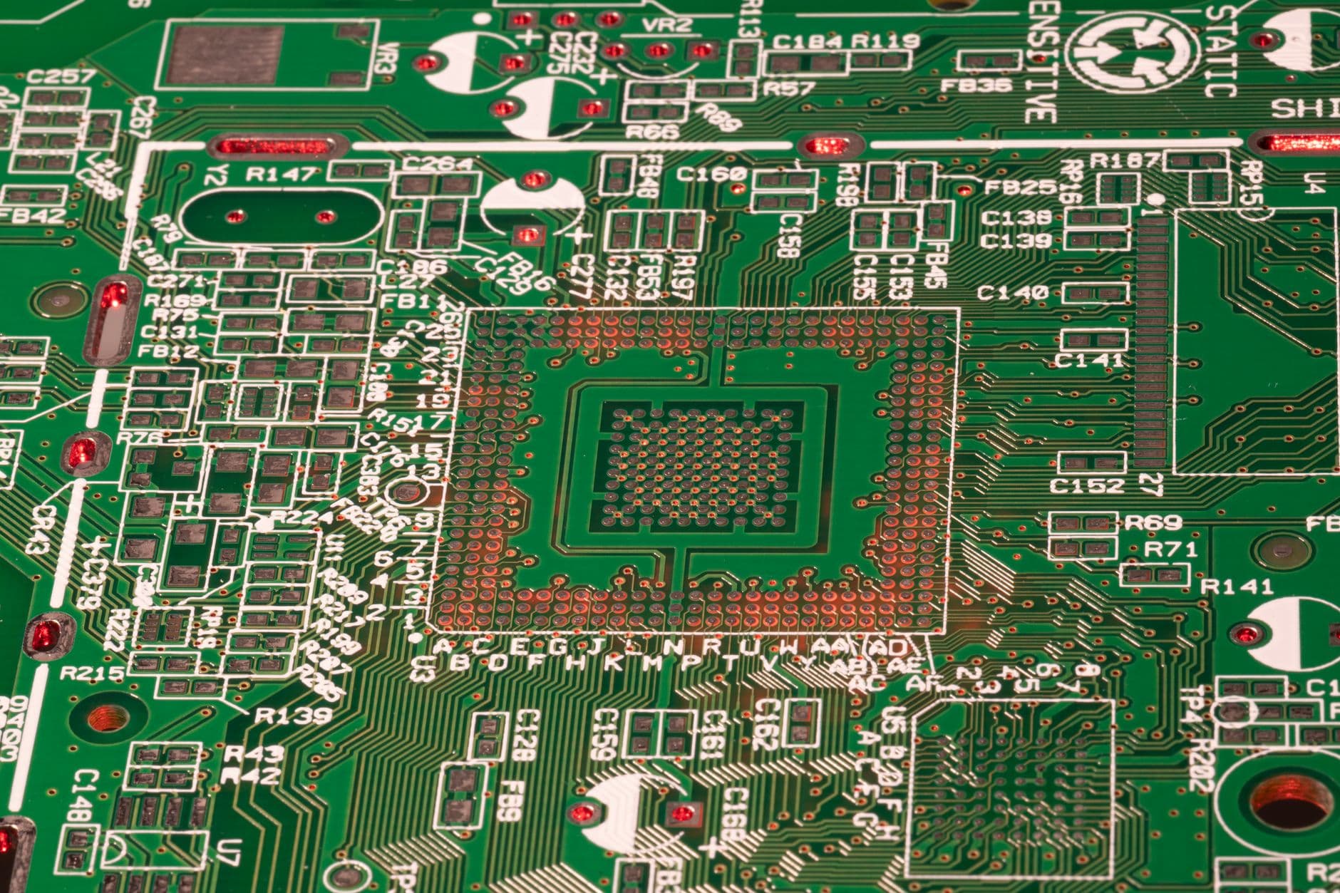
The Long, Expensive Walk Across the Motherboard
For decades, we’ve tolerated the von Neumann architecture like a long-distance relationship that everyone knows is failing. The CPU sits in its ivory tower, sending a telegram to the DRAM three inches away, asking for a single bit of data. The DRAM checks its notes, puts on its shoes, and walks that bit over the memory bus while the CPU sits around doing nothing but consuming power and contemplating its own existence. It’s a bottleneck so famous it has its own Wikipedia page, yet we’ve treated it as an unchangeable law of nature rather than a massive design flaw.
Samsung has decided that the solution is essentially to glue the memory to the processor's forehead. By shifting to custom logic bases for HBM4 and utilizing 16-layer stacking, they aren't just shortening the commute; they are merging the office and the bedroom. It turns out that when you’re trying to run a Large Language Model that consumes more electricity than a small European principality, waiting for a wire to carry data is considered an unacceptable luxury.
Sixteen Layers of Silicon Hubris
Stacking 16 layers of DRAM is the semiconductor equivalent of building a skyscraper out of lit matches. Each layer is a triumph of engineering, and each layer is also a thermal insulator for the one beneath it. Samsung is moving to a 4nm process for the logic die at the base of this stack, which is a lovely way of saying they are putting a very small, very hot stove underneath sixteen layers of blankets.
This isn't just a minor tweak in the spec sheet. By integrating the logic base—the brain that manages how data moves—directly into the HBM stack, Samsung is dismantling the traditional boundary between "thinking" and "remembering." We used to have clear lines. Now, we have a vertical monolith where the material physics of silicon are being pushed to their absolute breaking point. It’s a bold strategy for a species that still hasn't figured out how to make a printer work consistently.

Photo by Edward Jenner on Pexels
Thermodynamics is the New Moore’s Law
We spent fifty years obsessed with transistor density, treating Gordon Moore like a prophet while ignoring the guy in the corner screaming about the Second Law of Thermodynamics. Now that we’ve reached the point where we can cram billions of switches into a space the size of a fingernail, we’ve realized the problem isn't making them smaller; it’s stopping them from melting into a puddle of expensive slag. Heat dissipation is no longer a secondary engineering concern; it is the only concern.
When you stack 16 layers of memory on top of a logic die, you aren't just building a chip; you’re building a very efficient heater that occasionally does math. The bottleneck is no longer how fast we can switch a gate, but how fast we can move a phonon. We are literally fighting the vibration of atoms to ensure that an AI can generate a slightly more realistic picture of a cat in a tuxedo. It’s a noble pursuit for the pinnacle of human civilization.
The Vanishing Act of the Memory Bus
By the time HBM4 hits mass production around 2026, the concept of a "memory bus" will look as quaint as a horse-drawn carriage. When the logic is the base and the memory is the tower, the distance data travels is measured in microns, not millimeters. This sounds great until you realize that every single one of those microns is a potential failure point in a device that is being thermally cycled hundreds of times a day.
Samsung is betting that their custom 4nm logic dies can handle the overhead of managing this vertical city. It’s an incredibly complex dance of power delivery and signal integrity. If even one of those through-silicon vias (TSVs) decides to quit, the whole $10,000 unit becomes a very sophisticated paperweight. But hey, at least the latency was low while it lasted.
What This Actually Means
The move to HBM4 with integrated logic bases means the hardware industry has finally given up on the idea of general-purpose computing being efficient enough for the AI era. We are moving toward hyper-specialized, vertically integrated stacks where the hardware is literally molded to the shape of the software's demands. If you want to change how the memory talks to the processor later, too bad—it's baked into the physical structure of the silicon.
We are effectively trading flexibility for raw, unadulterated speed, and we’re doing it by pushing the limits of what solid-state matter can endure. The future of computing isn't about better code or smarter algorithms; it’s about who can build the best refrigerator to sit on top of a chip. It’s a fascinating, expensive, and deeply sweaty frontier.
Quick Answers
Why is 16-layer stacking such a big deal?
Because it doubles the capacity of previous generations while creating a thermal nightmare that engineers have to solve with increasingly exotic materials.
Does this mean my PC will get faster?
Unless you’re running a data center in your basement to train a neural network, no, this is strictly for the people who buy GPUs that cost more than your car.
What happens if it gets too hot?
The chip throttles itself, meaning you paid for 16 layers of performance but only get the speed of four because physics is a cruel mistress.
When will we see this in the real world?
Samsung is aiming for 2025/2026, assuming they can find a way to stack these things without them warping like a vinyl record left in the sun.